Commodore 16 internal function ROM
10 minute read Published: 2018-03-18For quite a while I had been wanting a member of the TED series. These are the computers from Commodore that employ the TED chip as their heart - the C16, the Plus/4 and their lesser known siblings, the C116, C264 and even C364.
What I really wanted was a Plus/4 because it just looks so good. A real cursor pad and better ergonomics than the C16. But an auction turned up and I got my hands on a untested C16 for an excellent price - it turned out to be fully functional (except a few broken traces on the keyboard matrix), and I upgraded it to 64 KiB and so on. What you'd usually do.
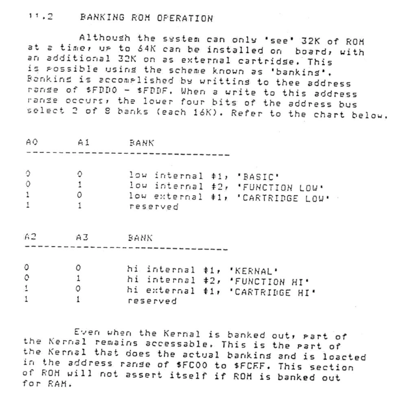
The TED computers share some common functions and are generally compatible with each other. After upgrading my C16 I had been wondering whether it would be possible to add internal function ROMs to the it. Its sibling, the Commodore Plus/4, ships with internal functions ROMs that provide the productivity software suite, but other, more interesting, options are also available. One thing they share is allowing for external function ROMs, on the Plus/4 you can have 32 KiB of internal ROMs (divided into 16 KiB "high" and "low") and the same externally in the cartridge port. The Commodore 16 only allows the external ROMs out of the box.
I wanted to find out if it would be possible to add something internally to the Commodore 16 as well.
Determining feasibility
With these kinds of things you can usually do whatever you dream up, but how much work is it? How much do you have to add to the machine to get it support internal function ROMs? A good place to start is comparing the Plus/4 and C16 schematics.
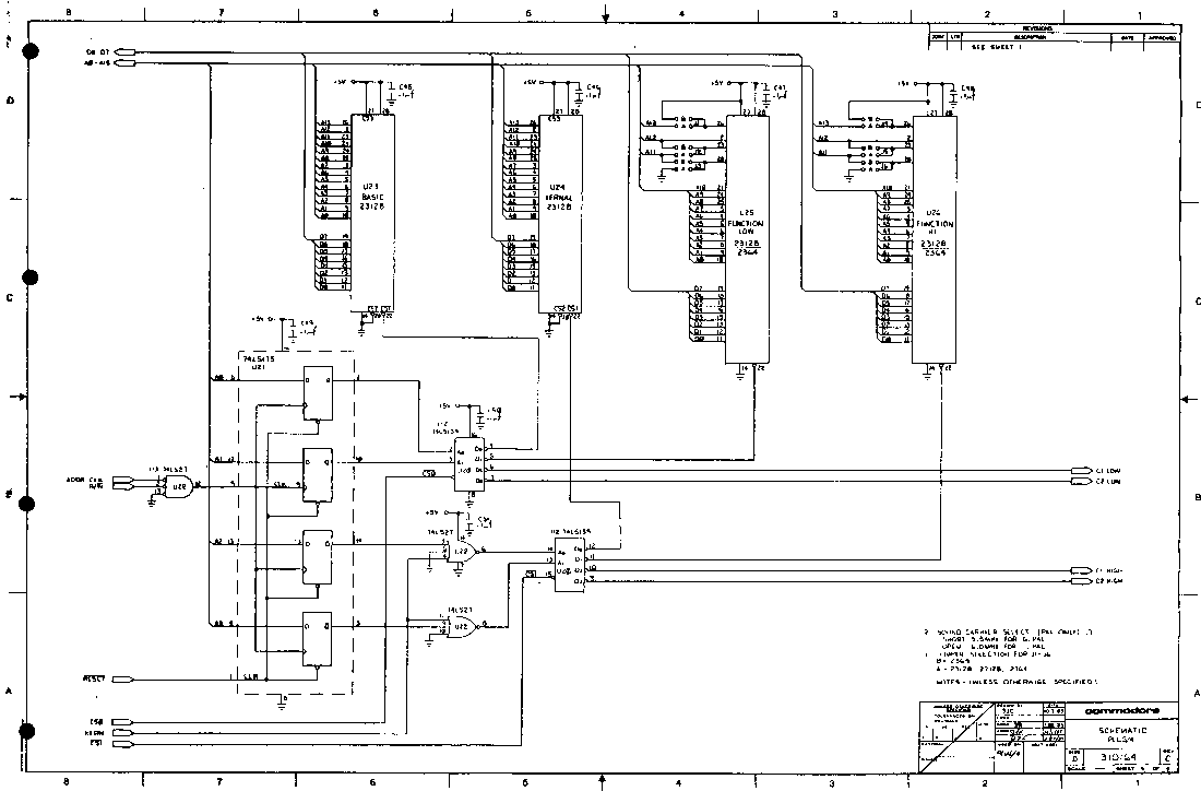
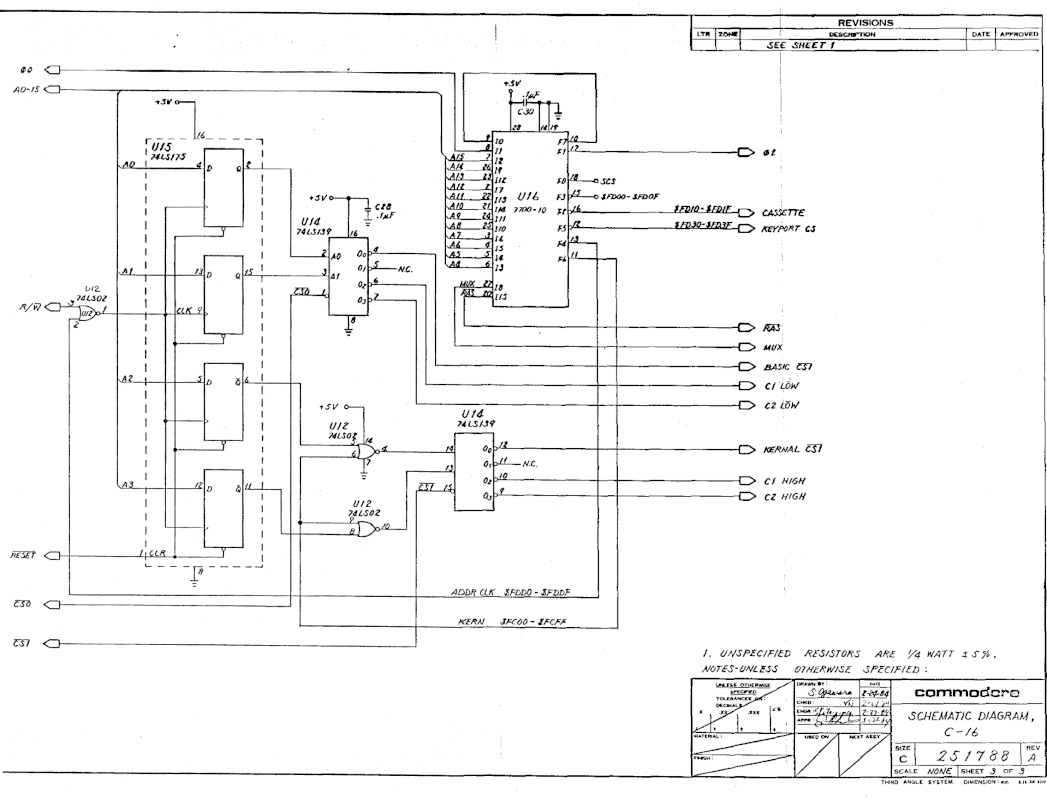
It looks like adding internal function ROMs will be as easy as putting EPROMs on the bus and wiring up the enable signals.
Implementation
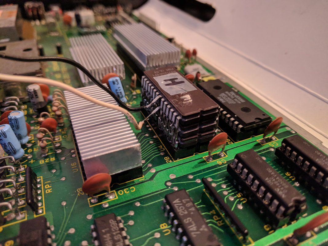
The first thing I want to do, is to make sure that pin 5 and 11 on U14 are, in fact, not connected to anything, like ground. Visual inspection of the board suggests that this is indeed the case. Using a multimeter it's possible to determine that the resistance from these pins to ground is 22 MΩ, which is perfectly normal from a logic output to ground. At this point I'm just going to go ahead and put some high and low function ROMs on the bus and connect them to the (almost certainly correctly generated) enable signals.
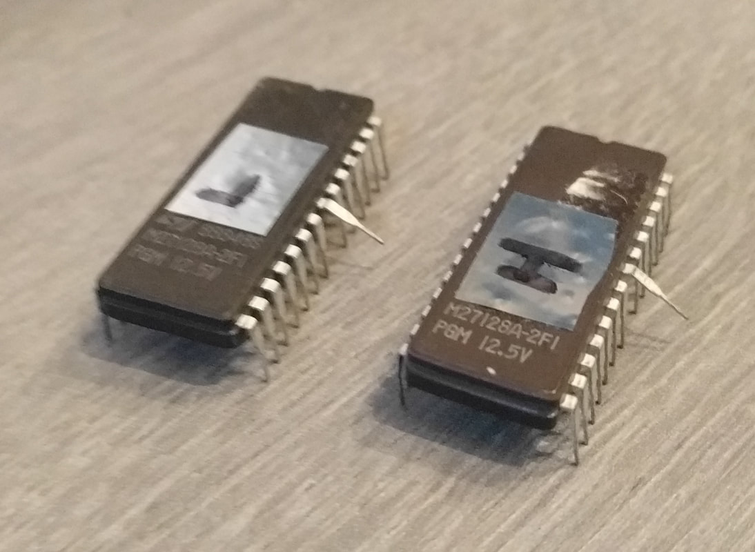
An easy way to get these on the bus is to stack them on top of the kernal ROM. By the way, there are some absolutely glorious examples out there of stacked chips. Anyway, stacking chips is easy, you just solder all the pins together, not connecting the ones you need to treat differently. I'm just interested in providing a different output enable signal (pin 22 on the 27128) to my new function ROMs, and I bend out those pins slightly.
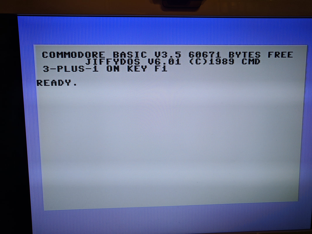
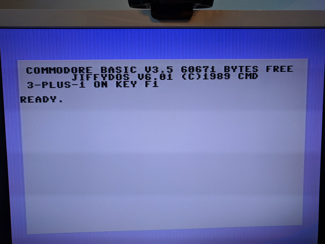
The moment has arrived. It looks good in theory, but does it actually work?
It's alive
Tidying up
OK, the C16 does in fact support internal function ROMs. All Commodore had to do was add a few IC sockets and wire them up, and users would have been able to plug in ROMs themselves. But the C16 was made to be cheap, and adding extra sockets would have increased the board size and supplying empty sockets for the tiny amount of users actually going to populate them? No, doesn't sound like a good idea.
But I am exactly the kind of person who wants to do that. And I would like to be able to easily burn new function ROMs, and having to desolder and resolder the EPROMs from my otherwise fantastic stack doesn't look particularly appealing. Ideally I'd also like to have the JiffyDOS kernal in the machine, and be able to switch in the old kernal if necessary.
At this point, making a board that plugs directly in to the kernal IC socket looks pretty easy. But a board with three or maybe four large IC's on it, sitting on top of a single socket, doesn't seem like a great long term solution, especially not if you're going to move the machine around.
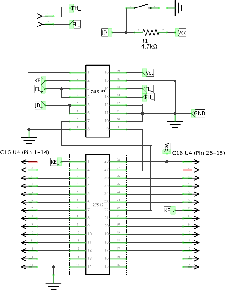
Basically I want to add three ROMs, and with the original kernal that's four 16 KiB ROMs. Which would fit nicely on a single 27512.
"Hmm," he wonders ...
Okay new goal - I decide I now want to be able to put four ROMs into one image like this:
$0000-$3FFF - JiffyDOS Kernal
$4000-$7FFF - Kernal
$8000-$BFFF - Function Low
$C000-$FFFF - Function Hi
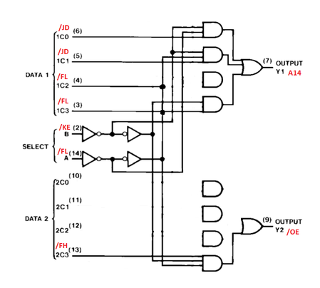
There's three output enable signals generated by the motherboard, I call them them /KE (kernal enable, supplied by the kernal IC socket), /FH (function high enable) and /FL (function low enable). An additional signal for selecting JiffyDOS or the regular kernal is needed, which will be supplied by a simple switch and pull up resistor combination, called /JD. All active low.
/JD = JiffyDOS enable (active low)
/KE = kernal enable (active low)
/FL = function low enable (active low)
/FH = function high enable (active low)
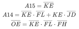
The motherboard provides A[13:0], but I need to generate the 27512's A14 and A15 signals somehow. With the ROM layout above, A15 is simply a select line that chooses between kernal or function rom. The A14 line selects between JiffyDOS and regular kernal when /KE is low, and between function ROM low and high when /KE is high. The last part can be done by just selecting /FL when /KE is high - it's not necessary to bring /FH into the equation, because when /FL is low, /FH is high, and when /FL is high, /FH is low.
The /OE signal is pretty simple in comparison, it needs to go low when any of /KE, /FL or /FH are low.
The formulas for these combinational circuits look like this:
This looks like more logic than I'm really hoping for. I'm going to need a few IC's from the 7400 series to do this. Unless ... A14 is basically a multiplexer. And multiplexers contain a fair amount of circuitry that can be configured to produce various useful functions if you drive unnecessary inputs high or low. Maybe there's one that could implement both A14 and /OE at the same time? There's comprehensive list of 7400 IC's on Wikipedia
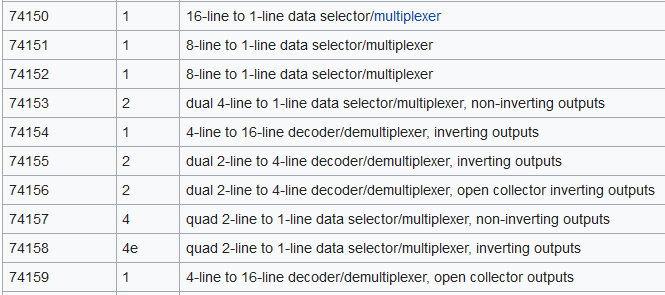
There's a couple of candidates here, those with two units are optimal (only two combinational circuits need to be implemented), and those ICs have the largest number of inputs. Of those the 74153 looks best, inverting outputs is not something I want at this point. What does the 74153 actually do?
That is quite an impressive amount of circuitry, already it looks much more promising than simple AND or OR gates.
I'll start out by defining that output Y1 is A14 and Y2 is /OE. The two strobe G1 and G2 signals (active high) are not needed, I'll tie those to GND.
Crucially, /KE and /FL are both necessary inputs to the signals I need to generate, so I'll assign those to the A and B inputs, as those are used in each unit.
For the A14 circuit, I'll tie 2C0, 2C1 and 2C2 to GND, which will drive some of the AND gates' outputs low. 2C3 will be connected to /FH, and the remaining AND gate will now perform the function of the A14 circuit, and the OR gate is just a pass through.
For the /OE circuit I'll assign /JD to 1C0 and 1C1, and /FL to 1C2 and 1C3. The third AND will always output 0, because its function includes FL*/FL which is always zero. The fourth AND gate performs /KE*/FL*/FL which trivially reduces to /KE*/FL. The first two AND gates perform FLKE/JD and /FLKE/JD. Since the outputs of these two are OR'ed together, the FL and /FL inputs can be ignored, and together these two AND gates perform the KE*/JD function.
Another experiment
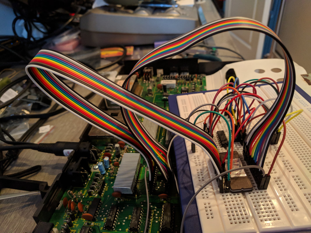
The breadboard implements a circuit much like this one, but the completed board is a topic for another post.